Nanoscale displacement sensor
The ability to measure very precise alignments and displacements is a key requirement for many steps in semiconductor fabrication and manufacturing, for example, during lithography or wafer bonding. Using small nanoparticles, exhibiting a Huygens dipole coupled to crossed Photonic crystal waveguides we have now shown that light can be used to measure displacements of a few nm, beyond the accuracy of many current alignment systems.
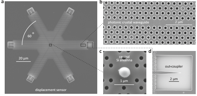
Together with our colleagues from the Max Planck Institute for the Science of Light in Erlangen, we developed a three-way waveguides crossing with a nanoparticle on its centre. If there is a displacement between the centre of an optical beam and the nanoparticle, then the light will couple into the waveguides with a directionality which we can measure using the same objective used to excite the Huygens dipole. By measuring the different optical power output from each end of the waveguides we can work out the displacement between the nanoparticle and the axis of the incident beam.
The work has now been published in Nature Communications. Here is a link to the full article.