Nanometer precision displacement sensors
Silicon photonics, the use of light to transmit and process information, has become increasingly popular over the last few years due to its high data transmission rates and compatibility with existing integrated circuit technology. However, one limitation of this technology is the lack of on-chip integrated devices for measuring alignment and displacement, resulting in high device costs. This has made high-resolution displacement sensing challenging, even in applications where it would be useful, such as the packaging of nanophotonic devices.
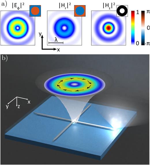
Fortunately, we have developed a new device that addresses this limitation. The device uses a tightly focused beam of light to excite a silicon cylinder on an SOI platform, surrounded by silicon waveguides. The displacement between the beam and cylinder affects the directionality of waveguide coupling, resulting in a unique optical output that directly corresponds to both the direction and magnitude of displacement. This allows for nanometer-precision measurements and highly precise alignment in nanolithography systems.
This device represents a significant advancement in silicon photonics and is an exciting development for a variety of applications, such as sensing and telecommunications. Moreover, the potential for time-resolved position sensing and compensation of environmental mechanical noise makes this technology even more promising for future applications. If you want more information read out paper in APL Photonics.